Another aspect of the behavior of electronic devices which is of much interest to circuit designers is the small-signal ac response of the device. This is the response of the device to a small sinusoidal voltage imposed upon a generally much larger dc bias voltage. That is, one seeks to evaluate the effect of a small perturbation on a far-from-equilibrium steady state. This is a rather different problem from that treated by the linear response theory of statistical physics (Kubo, 1957), which seeks to evaluate the effect of small perturbations on an equilibrium state. A perturbation expansion of the present kinetic theory may be readily obtained to evaluate the small-signal ac response of our model RTD (Frensley, 1987b, 1988a; Mains and Haddad, 1988b). Let us assume that the potential of the system varies as
where  denotes the complex conjugate,
  is the dc potential
including the heterostructure and the large bias voltage,
is the dc potential
including the heterostructure and the large bias voltage,  is the potential due to the small ac voltage, and
  is a
perturbation parameter introduced solely to keep track of the order of
the perturbation (and is ultimately set equal to unity). We should
expect that the current induced in the external circuit can be expanded
as
is a
perturbation parameter introduced solely to keep track of the order of
the perturbation (and is ultimately set equal to unity). We should
expect that the current induced in the external circuit can be expanded
as
where  and
and  are the total voltages applied, e being the charge
of the electron. The coefficients of (5.61) describe different
aspects of the ac response: y is the linear admittance,
the amount of rectification of the sinusoidal waveform is given by
are the total voltages applied, e being the charge
of the electron. The coefficients of (5.61) describe different
aspects of the ac response: y is the linear admittance,
the amount of rectification of the sinusoidal waveform is given by
 , and the amount of second-harmonic generation is given by
 . Note that at
  these coefficients are just the
derivatives of the
these coefficients are just the
derivatives of the  curve:
  and
and  . The coefficients of (5.61) at an
arbitrary frequency may be obtained from the corresponding components of
the Wigner function. To do this we write the Liouville operator as
. The coefficients of (5.61) at an
arbitrary frequency may be obtained from the corresponding components of
the Wigner function. To do this we write the Liouville operator as
The Wigner function can be expanded (to second order in  ) as
) as
Inserting (5.62) and
(5.63) into the Liouville equation and collecting terms of equal
frequency and order in  leads to these equations:
where  is obtained from (4.56). (The denominators of this
perturbation series look a bit unfamiliar, with expressions of the form
is obtained from (4.56). (The denominators of this
perturbation series look a bit unfamiliar, with expressions of the form
 rather than
  . The
reason for this is that we have mixed the quantum-mechanical convention
for the time dependence,
. The
reason for this is that we have mixed the quantum-mechanical convention
for the time dependence,  , with the convention
used in electronics,
, with the convention
used in electronics,  . While a consistently
quantum-mechanical notation would produce more conventional expressions,
it would also produce a great deal of confusion when we examine the
imaginary parts of the response to determine whether they resemble
capacitances or inductances.) The superoperator resolvent expressions
in (5.64)--(5.66) are readily evaluated with the same
algorithms used to solve the steady-state and transient problems.
. While a consistently
quantum-mechanical notation would produce more conventional expressions,
it would also produce a great deal of confusion when we examine the
imaginary parts of the response to determine whether they resemble
capacitances or inductances.) The superoperator resolvent expressions
in (5.64)--(5.66) are readily evaluated with the same
algorithms used to solve the steady-state and transient problems.
Evaluating the expectation value of the current density J for any
of the terms of  gives the conduction current as a function of
position q:
gives the conduction current as a function of
position q:
The current induced in the external circuit by this conduction current
within the device is obtained by invoking the Shockley-Ramo theorem
(Shockley, 1938; Ramo, 1939). We will approximate the properties of the
doped contacting layers as ideally metallic conductors bounded by
interfaces to the higher-potential barrier layers at  and
and
 . The Shockley-Ramo theorem then takes the form:
where A is the area of the device. The coefficients of the expansion
of  (5.61) are thus given by:
It should be emphasized that these expressions represent only the conduction current component; the displacement current must be added to them to obtain a complete description of the behavior of the device.
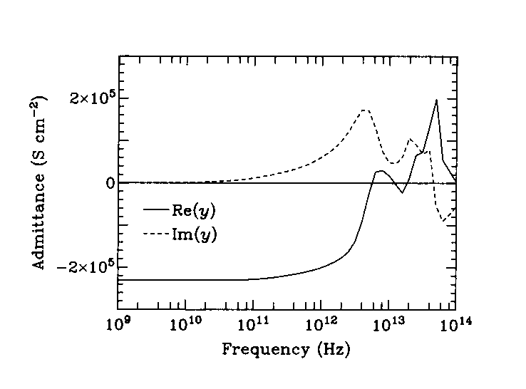
Figure 17. Small-signal ac response of the resonant-tunneling diode for a dc bias of 0.17 V, which places the device in the middle of the negative-resistance region. The device conductance (the real part of the admittance, solid line) is negative at lower frequencies, with a value equal to that expected from the derivative of the dccurve. The negative conductance decreases in magnitude and becomes positive at a few THz. The complex behavior at higher frequencies is an indication that optical transitions are becoming important. The susceptance (imaginary part of the admittance, dashed curve) has the same sign as a capacitance and is due to the effects of electron storage in the quantum well. These quantities reflect only the conduction current and do not include the displacement current through the parasitic capacitance of a real device. This displacement current would prevent observation of the higher-frequency effects in a realistic experimental situation.
The linear admittance y of the present RTD model was evaluated
using (5.64) and (5.70) at a
bias of 0.17 V (in the middle of the negative-resistance region), as a
function of frequency over the GHz and THz regions. The results are
plotted in Fig. 17. The conductance  is negative
at lower frequencies, as we would expect from the dc results. This
negative conductance ``rolls off'' and becomes positive at about 6 THz,
which is therefore the maximum frequency of oscillation of the intrinsic
device (not including parasitic effects). The susceptance
is negative
at lower frequencies, as we would expect from the dc results. This
negative conductance ``rolls off'' and becomes positive at about 6 THz,
which is therefore the maximum frequency of oscillation of the intrinsic
device (not including parasitic effects). The susceptance  is
positive and proportional to
is
positive and proportional to  at lower frequencies, which is the
behavior of a capacitance. Recall, however, that the displacement
current which flows through the geometrical device capacitance is not
included in this calculation. The result that
at lower frequencies, which is the
behavior of a capacitance. Recall, however, that the displacement
current which flows through the geometrical device capacitance is not
included in this calculation. The result that  is somewhat
surprising, since the most obvious reactive effect in electron transport
at high frequencies is the electron inertia, which leads to
is somewhat
surprising, since the most obvious reactive effect in electron transport
at high frequencies is the electron inertia, which leads to
 resembling that of an inductor with
  negative
(Champlin, Armstrong, and Gunderson, 1964). The initial calculations of
the admittance by the present author (Frensley, 1987b, 1988a) gave
negative
negative
(Champlin, Armstrong, and Gunderson, 1964). The initial calculations of
the admittance by the present author (Frensley, 1987b, 1988a) gave
negative  due to a programming error, and the electron-inertia
explanation was proposed in those papers. During the preparation of the
present work the error was discovered, and correcting it brings the
results into agreement with those obtained by Mains and Haddad
(1988b), who obtained positive
due to a programming error, and the electron-inertia
explanation was proposed in those papers. During the preparation of the
present work the error was discovered, and correcting it brings the
results into agreement with those obtained by Mains and Haddad
(1988b), who obtained positive  . Thus, the electron inertia does
not explain the behavior of
. Thus, the electron inertia does
not explain the behavior of  , and an alternative
explanation must be sought. A key piece of evidence is provided by
evaluating the admittance of structures with either one energy
barrier or none, in addition to the double-barrier structure. These structures
do indeed show negative (inductive)
, and an alternative
explanation must be sought. A key piece of evidence is provided by
evaluating the admittance of structures with either one energy
barrier or none, in addition to the double-barrier structure. These structures
do indeed show negative (inductive)  , presumably due to electron
inertia. The capacitive
, presumably due to electron
inertia. The capacitive  is thus uniquely associated with the
double-barrier structure and therefore must reflect the confinement of
electrons in the quantum well. The idea that electron storage in a
quantum well could be represented as a capacitance was proposed by Luryi
(1985), but he identified this capacitance with the geometrical
capacitance of the device, through which the displacement current flows.
The storage capacitance inferred from the present calculation is 1--2
orders of magnitude smaller than the geometrical capacitance.
is thus uniquely associated with the
double-barrier structure and therefore must reflect the confinement of
electrons in the quantum well. The idea that electron storage in a
quantum well could be represented as a capacitance was proposed by Luryi
(1985), but he identified this capacitance with the geometrical
capacitance of the device, through which the displacement current flows.
The storage capacitance inferred from the present calculation is 1--2
orders of magnitude smaller than the geometrical capacitance.
Figure 18. Nonlinear response of the resonant-tunneling diode at a dc bias of 0.13 V, at the peak of thecurve. The rectification coefficient (solid line) shows a resonant enhancement near 6 THz.
The rectification and second-harmonic generation coefficients
 and
and  were evaluated using (5.65),
(5.66), (5.71), and (5.72) at a bias of 0.13 V
(the top of the current peak). The moduli of these quantities are shown
in Fig. 18. While
were evaluated using (5.65),
(5.66), (5.71), and (5.72) at a bias of 0.13 V
(the top of the current peak). The moduli of these quantities are shown
in Fig. 18. While  decreases at higher
frequencies,
decreases at higher
frequencies,  shows a resonant enhancement over the frequency
range of 1 to 8 THz. This is quite interesting, because
shows a resonant enhancement over the frequency
range of 1 to 8 THz. This is quite interesting, because  was
measured by Sollner et al. (1983) at a frequency of 2.5 THz. The
experimental data show that for most bias voltages
was
measured by Sollner et al. (1983) at a frequency of 2.5 THz. The
experimental data show that for most bias voltages  exceeds the dc
  , indicating that the magnitude
of
, indicating that the magnitude
of  must increase in this frequency range. On the other hand,
the rectification process in the RTD has been recently analyzed by
Wingreen (1990), using a transmission-coefficient approach. He found no
evidence of enhancement, only a decrease in
must increase in this frequency range. On the other hand,
the rectification process in the RTD has been recently analyzed by
Wingreen (1990), using a transmission-coefficient approach. He found no
evidence of enhancement, only a decrease in  as the frequency is
raised. One difference between Wingreen's calculation and that based
upon (5.65) is that the former includes the effects of only one
resonant level, whereas the latter includes all such levels. This
suggests that the enhancement of
as the frequency is
raised. One difference between Wingreen's calculation and that based
upon (5.65) is that the former includes the effects of only one
resonant level, whereas the latter includes all such levels. This
suggests that the enhancement of  might involve transitions
between resonant levels, though the frequency of the transition between
the lowest two levels in the present example is 60 THz, which argues
against this notion. This illustrates one of the problems with a kinetic
approach which incorporates all physical processes:
Such an approach provides little guidance when one desires to identify
that process which is the cause of some particular effect.
might involve transitions
between resonant levels, though the frequency of the transition between
the lowest two levels in the present example is 60 THz, which argues
against this notion. This illustrates one of the problems with a kinetic
approach which incorporates all physical processes:
Such an approach provides little guidance when one desires to identify
that process which is the cause of some particular effect.
Figure 19. Linear component of the ac current density (divided by the applied ac voltage and thus expressed as an admittance) as a function of frequency and position. At lower frequencies the current density is spatially uniform, but strong nonlocal effects develop as the frequency is increased. This is a characteristic of the transition from electronic to optical behavior. The prominent peak incentered in the quantum well at 50 THz is due to quantum transitions between the two lowest resonant levels.
It is particularly interesting to look at  as a function of both frequency and position q. This is plotted in
Fig. 19. At frequencies below a few THz the
current is independent of position, as one would expect in an electron
device. As the frequency increases above this value, the ac current
density becomes strongly nonuniform, indicating that the response of the
current to the applied potential is strongly nonlocal. A particularly
prominent peak occurs in
as a function of both frequency and position q. This is plotted in
Fig. 19. At frequencies below a few THz the
current is independent of position, as one would expect in an electron
device. As the frequency increases above this value, the ac current
density becomes strongly nonuniform, indicating that the response of the
current to the applied potential is strongly nonlocal. A particularly
prominent peak occurs in  at a frequency of 50 THz and
centered within the quantum well. The positive value of the conductance
in this peak indicates that the in-phase current density is locally
large, so this part of the device is absorbing power from the ac
electric field. The obvious explanation for this absorption is that the
peak reflects quantum transitions
between the two lowest resonances in the well. A
transmission-coefficient calculation indicates that, for the present
example, these states are separated in energy by 0.248 eV, for which the
corresponding photon frequency is 60 THz. The small discrepancy in
predicted frequencies is presumably attributable to the effect of the
Markov assumption in the kinetic theory, as in the case of the
at a frequency of 50 THz and
centered within the quantum well. The positive value of the conductance
in this peak indicates that the in-phase current density is locally
large, so this part of the device is absorbing power from the ac
electric field. The obvious explanation for this absorption is that the
peak reflects quantum transitions
between the two lowest resonances in the well. A
transmission-coefficient calculation indicates that, for the present
example, these states are separated in energy by 0.248 eV, for which the
corresponding photon frequency is 60 THz. The small discrepancy in
predicted frequencies is presumably attributable to the effect of the
Markov assumption in the kinetic theory, as in the case of the
 curves. Figure 19 is
interesting because it gives us a view of the transition of a single
system from the domain of electronics to that of optics.
curves. Figure 19 is
interesting because it gives us a view of the transition of a single
system from the domain of electronics to that of optics.
In addition to the these effects, the irreversible open-system models have been applied to investigations of the effects of phonon scattering, as described in Appendix 14, and the self-consistent potential in the RTD, as described in Appendix 9. The various applications of open-system kinetic theory to RTDs clearly demonstrate the value of this approach, in spite of the existence of several unresolved mathematical issues which will be explored in the next section.