HSPICE by Synopsys
0. Simulation with HSPICE
Once generate netlist file, You can simulate by using HSPICE.
Start HSPICE
Tip
If you need to use both Cadence tools and Synopsys tools, use them in different terminals (tabs), e.g. use Cadence in one terminal, and use HSPICE in another, after sourcing proper profiles.
Go to your HSPICE working directory first.
cd ~/cad/spice
source the Synopsys profile:
. /proj/cad/startup/profile.synopsys_2018
To run hspice you enter this command:
hspice YOUR_SPICE_FILE.sp
If you want to get the output log, you can do:
hspice YOUR_SPICE_FILE.sp > YOUR_SPICE_FILE.out
You can check the output log if there's any warning or error.
If it said job concluded, it means simulation running successfully, otherwise, if it said job aborted or some other message, your simulation didn't finish and you won't see any output files.
Your transient analysis results waveform is stored in YOUR_SPICE_FILE.tr0. You can use the waveform viewer (WaveView) to open it.
Your transient analysis measurement results is stored in YOUR_SPICE_FILE.mt0. You can use any text editor to read it, you can also use WaveView if sweep with some parameter.
Note
Make sure the first line is empty or a comment($....), it will be ignored by HSPICE
This is example HSPICE setup file.
$example HSPICE setup file

$transistor model
.include "/proj/cad/library/mosis/GF65_LPe/cmos10lpe_CDS_oa_dl064_11_20160415/models/YI-SM00030/Hspice/models/design.inc"
.include "inv.pex.sp"


.option post runlvl=5

xi GND! OUT VDD! IN inv

vdd VDD! GND! 1.2v
vin IN GND! pwl(0ns 1.2v 1ns 1.2v 1.05ns 0v 6ns 0v 6.05ns 1.2v 12ns 1.2v)
cout OUT GND! 100f

$transient analysis
.tr 100ps 12ns
$example of parameter sweep, replace numeric value W of pfet with WP in invlvs.sp
$.tr 100ps 12ns sweep WP 1u 9u 0.5u

.measure tran trise trig v(IN) val=0.6v fall=1 targ v(OUT) val=0.6v rise=1 $measure tlh at 0.6v
.measure tran tfall trig v(IN) val=0.6v rise=1 targ v(OUT) val=0.6v fall=1 $measure tpl at 0.6v
.measure tavg param = '(trise+tfall)/2' $calculate average delay
.measure tdiff param='abs(trise-tfall)' $calculate delay difference
.measure delay param='max(trise,tfall)' $calculate worst case delay

$ method 1
.measure tran iavg avg i(vdd) from=0 to=10n $average current in one clock cycle
.measure energy param='1.2*iavg*10n' $calculate energy in one clock cycle
.measure edp1 param='abs(delay*energy)'

$ method 2
.measure tran t1 when v(IN)=1.19 fall=1
.measure tran t2 when v(OUT)=1.19 rise=1
.measure tran t3 when v(IN)=0.01 rise=1
.measure tran t4 when v(OUT)=0.01 fall=1
.measure tran i1 avg i(vdd) from=t1 to=t2 $average current when output rise
.measure tran i2 avg i(vdd) from=t3 to=t4 $average current when output fall
.measure energy1 param='1.2*i1*(t2-t1)' $calculate energy when output rise
.measure energy2 param='1.2*i2*(t4-t3)' $calculate energy when output fall
.measure energysum param='energy1+energy2'
.measure edp2 param='abs(delay*energysum)'

.end
.include invlvs.sp include the circuit file generated by PEX or created manually.
xi in out inv instance the subckt
-
xi : instance name of your choice
-
in out : IO ports, please follow the same order as the IOs in your netlist (ports are mapped by the order)
-
inv : subckt name of the subckt you are calling
Please create your own spice file from the example, you may need add your own input sources and device
Definitions of waveforms

Slew rate: the time period for a signal between 0.1*vdd and 0.9*vdd.
tLH: delay from input 50% to output 50% when output is rising.
tHL: delay from input 50% to output 50% when output is falling.
Tips
Measuring Average power for a period by HSPICE. Energy E = Vdd * Iavg * (end Time - start Time).
Usually we care about Energy per operation, and there are two methods to calculate the Energy per operation:
-
Measure the Iavg for one or N cycle time (includes the rise and fall edge) and use the
Energy = Vdd * Iavg * N * Tcycle -
For output rising edge, measure the Iavg during the time from
T1[start of the input falling edge, e.g. v(in)=1.19 fall=1] toT2[end of the output rising edge, e.g. v(out)=1.19 rise=1], such thatEnergy_rise = Vdd * Iavg * (T2-T1), do the same thing for output falling edge and getEnergy_fall = Vdd * Iavg * (T4-T3).
You will find that energy in method 1 is a little bigger than the energy in method 2 (yet very close) because the current besides the transition time is not zero but very small. For the purpose of accuracy, the method 1 is preferred. The longer time you use for measuring the Iavg and calculating energy, the more accurate result you can get.
Transistor models
IBM 130nm
.include "/home/cad/kits/IBM_CMRF8SF-LM013/IBM_PDK/cmrf8sf/V1.2.0.0LM/HSPICE/models/model013.lib_inc"
GF 65nm
.include "/proj/cad/library/mosis/GF65_LPe/cmos10lpe_CDS_oa_dl064_11_20160415/models/YI-SM00030/Hspice/models/design.inc"
If you generate netlist from schematic instead of layout, and your netlist is like:
.subckt inv in out

xt1 out in 0 0 nfet l=120e-9 w=800e-9 nf=1 m=1 par=1 ngcon=1 ad=440e-15 as=440e-15 pd=2.7e-6 ps=2.7e-6 nrd=225e-3 nrs=225e-3 rf_rsub=1 plnest=-1 plorient=-1 pld200=-1 pwd100=-1 lstis=1 lnws=0 rgatemod=0 rbodymod=0 panw1=0 panw2=0 panw3=0 panw4=0 panw5=0 panw6=0 panw7=0 panw8=0 panw9=0 panw10=0 sa=550e-9 sb=550e-9 sd=0 dtemp=0

xt0 out in vdd! vdd! pfet l=120e-9 w=2.5e-6 nf=1 m=1 par=1 ngcon=1 ad=1.375e-12 as=1.375e-12 pd=6.1e-6 ps=6.1e-6 nrd=72e-3 nrs=72e-3 rf_rsub=1 plnest=-1 plorient=-1 pld200=-1 pwd100=-1 lstis=1 lnws=0 rgatemod=0 rbodymod=0 panw1=0 panw2=0 panw3=0 panw4=0 panw5=0 panw6=0 panw7=0 panw8=0 panw9=0 panw10=0 sa=550e-9 sb=550e-9 sd=0 dtemp=0

.ends inv
You would have to change the xt0 xt1 to mt0 mt1 for simulation in HSPICE.
Please read thought EVERY Section below, if you are not familiar with HSPICE.
1. Getting Start
Introduction
Hspice is a circuit simulator. It can take input circuit description files and produce output files describing the requested simulation. For beginners, the best way to learn Hspice is to do a simple simulation. After running a simple simulation, you will learn
- how to create a Hspice input file
- run Hspice
- inspect the output
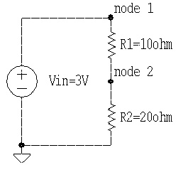
Okay, let's start with a simple circuit. This circuit is simple, by inspection you know how the circuit works. By naming the nodes as shown in the figure, an input file to Hspice to simulate the circuit can be like this:
* sample circuit
Vin 1 0 3
R1 1 2 10
R2 2 0 20
.END
By using your favorite text editor to create the above file in *.sp, you are ready to run Hspice simulation.
Input File
In the above example file, the title line (first line) starts with *, which indicates a comment line. It is necessary that the last line should end with .END statement, which computes the description of the entire circuit including any simulation controls. Any text that follows the .END statement is treated as a comment and has no effect on the simulation.
All of the circuit elements are connected by circuit nodes. Every circuit file must have a reference node, the ground node, and every other node in the circuit file must have a DC path to ground. Along with a ground node, all terminals must be connected to at least one other terminal. This is a precaution against dangling wires.
The circuit file for our example uses only two-terminal devices, a voltage source and two resistors. A seperate line is used to describe each element in the circuit. The basic syntax is
name node node [node ... ] value
There are no one-terminal devices in Hspice. Devices more than two terminals use basically the same form, but with more optional [node ... ] items. The devices' values are a number that describes the size of the device.
Apart from *, Hspice also allows you to insert comments on any line by starting the comment with a dollar sign $. Everything on the line after $ is ignored.
Information on describing both passive and active devices are given in section 2.
Examples
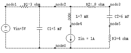
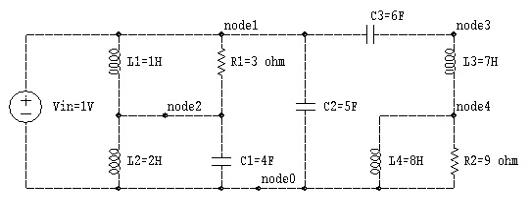
Okay, let's do some examples. Here are three simple RLC circuits, let's see if you have the right format for the input file.
Example 1:

Hspice file:

Example 2:
Hspice file:

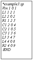
Example 3:
Hspice file:
2. Device Descriptions
Passive Elements
This section describes passive elements and they are resistor, inductor, and capacitor. Assorted magnetic elements are supported by Hspice but they are not included.
Resistors, inductors, and capacitors come in two types:
- a simple, linear element with a value and some dependence on temperature, initialization, and scaling
- an element that refers to a model statement
Using the set of passive elements and models statements available, you can construct a wide range of board and integrated level designs. To use a particular element, an element statement is needed. It specifies the type of element used. It has fields for the element name, the connecting nodes, a component value and optional parameters. The general form is shown below:
name node1 node2 ... nodeN [model reference] value [optional parameters]
Element parameters within the element statement describes the device type, device terminal connections, associated model reference, element value, DC initialization voltage or current, element temperature, and parasitic.
As you might have guessed, we can specify these three passive devices merely by using the first letter of the device name.
- Rxxx for resistor
- Lxxx for inductor
- Cxxx for capacitor
Fortunately, most of the resistors, inductors, and capacitors we use on lab-bench are nearly ideal and for our purposes we can consider them to be ideal. To specify the device in the circuit file, we can include the name of the device, how it is connected into the circuit, and its value. Hspice uses the basic electrical units for voltage (volts) and current (amperes) and uses the basic electrical units for device values: ohms, farads, and henries. Here are some example devices:
R12 3 4 5k $a 5-kiloohm resistor connected to node 3 and node 4
C7 9 10 3u $a 3-microfarad capacitor connected to node 9 and node 10
L5 6 8 1m $a 1-milihenry inductor connected to node 6 and node 8
Other Elements
This section will describe the use of elements like, diode, BJT, JFET, MESFET, and MOSFET.
Independent Sources
To simulate your circuits you will need some way to tell Hspice what is "exciting" or supplying electrical power to the circuit. We specify these sources in a way similar to the passive devices described earlier: name, connecting nodes, and value. As you might have expected
- Vxxx is a voltage source
- Ixxx is a current source
Using basic electrical units, the following examples are easy to understand:
Vin 1 0 3
Iin 2 0 5m
A voltage source is like a battery, or lab-bench power supply. Using positive current convention, current flows out from the first node, through the circuit and then into the second node. A current source provides a fixed value of current to the circuit. However, its current flows into the first node, through the source, and then out of the second node. This is the opposite direction of the voltage source.
Dependent Sources
Controlled sources measure voltage or current and use the measured value to control their output, which can be either a voltage or current. For linear controlled sources, we have the following four sources:
- voltage controlled voltage source (VCVS) E
- current controlled current source (CCCS) F
- voltage controlled current source (VCCS) G
- current controlled voltage source (CCVS) H
These four sources are devices, are given by E, F, G, and H. Similar to independent sources, they can be specified using: name, connecting nodes, and the transforming polynomial.
In the most simplest form, an example of a VCVS
E1 7 5 1 2 10
is a voltage source, with output nodes of 7 and 5 (the positive current is flowing out of the connection to node 7), and where the output coltage is controlled bu the voltage present at node 1 and 2, with a simple multiplying gain of a factor of 10. Instead of controlling nodes, the syntax includes the name of the V devices that has the controlling current. For instance
F4 3 5 V2 5
is a current source whose output current is 5 times the current flowing through V2.
Parameters and Functions
Sometimes electronic circuits are often designed through the use of formulas. In creating a design, you may not want to commit to particular component values because you have only general contraits for the circuit when you are getting started. These design values you want to specify will be parameters, which can be defined b the following form:
.PARAM name=value ...
You may define more than one parameter on the same line.
Let's say we want a voltage divider to provide 20% of the input voltage and load the input by 50 kilo-ohm, we can define the parameters as
.PARAM load = 50k
.PARAM ratio = 0.2
Out divider can be defined with following lines,
Ra in out "load*(1-ratio)"
Rb out gnd "load*ratio"
One wawy to build complicated formulas is to use a macro-like expansions in your formulas. These "macros" are defined using the .Func statement, which has the following form:
.FUNC name (arg ...) {body}
where the use of name, with its arguments, will be replaced with the body of the .FUNC definition. An example function is shown below.
.FUNC top(load,ratio) {load*(1-ratio)}
Ra in out {top(load,ratio)}
3. Input Sources Description
You may recall that the independent sources and current sources has the statement form:
name node node value
where value was the DC or AC voltage of current level, depending on the device type. A more complete representation of the input source statement is
name node node [DC_value] [AC_value] [transient_value]
The DC value will be used for the operatioing point analysis and DC sweep. The AC value may combine with DC value to set the operating point for the small-signal analysis. The transient value will override the other specifications only during the transient analysis. If transient value is not specified, the DC value will be used and the source is assumed to remain constant during the simulation.
The transient value portion of the statement has several forms, one for each type of waveform. The most commonly used forms are:
- PWL - piecewise linear waveform
- PULSE - pulse waveform
- SIN - sinusoidal waveform
- EXP - exponential waveform
During the transient analysis, all of the independent voltage sources having a transient specification will be activated. The remaining independent sources will maintain the value of the DC specification, or zero if there is no DC specification.
Piecewise Linear Waveform (PWL)
General form
PWL (T1 V1 T2 V2 T3 V3 ... Tn Vn ... )
Example
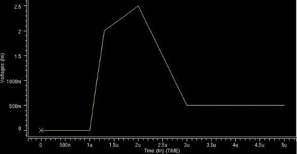
V3 10 5 PWL(0us 0V 1us 0V 1.3us 2V 2us 2.5V 3us 0.5V 3.4us 0.5V)
or
V3 10 5 PWL(0us,0V 1us,0V 1.3us,2V 2us,2.5V 3us,0.5V 3.4us,0.5V)
| PWL parameter | Default Value | Units |
|---|---|---|
| Tn - time at corner | none | second |
| Vn - voltage at corner | none | volt |
The PWL form describes a piecewise linear waveform. Each pair of time-voltage value pairs specifies a corner of the waveform. The voltage at times between corners is the linear interpolation of the voltage at the corners. If the first pair's time is not zero, then the source's DC voltage will be used as the initial value. If the simulation continues beyond the last pair's time, then that pair's voltage will be maintained for the remainder of the simulation.
Pulse Waveform (PLUSE)
General form
PULSE (V1 V2 Td Tr Tf Pw Period)
Example
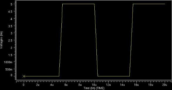
VSW 10 5 PULSE (0V 5V 5us 0.5us 0.5us 4.5us 10us)
| PULSE parameter | Default Value | Units |
|---|---|---|
| V1 - initial voltage | none | volt |
| V2 - peak voltage | none | volt |
| Td - initial delay time | 0 | second |
| Tr - rise time | Tstep | second |
| Tf - fall time | Tstep | second |
| Pw - pulse width | Tstep | second |
| Period - pilse period | Tstep | second |
The PULSE form causes the voltage to start at V1 and stay there for Td1 seconds. Then, the voltage goes linearly from V1 to V2 for Pw seconds. The, the voltage goes linearly from V2 back to V1 during the next Tf seconds. The voltage stays at V1 for Period-Tr-Pw-Tf seconds, and then the cycle is repeated.
Sinusoidal Waveform (SIN)
General form
SIN (Vo Va Freq Td Df Phase)
Example
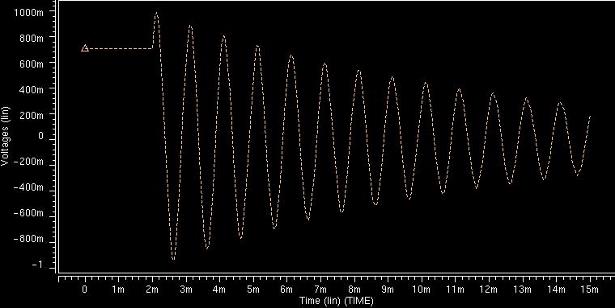
VSIG 10 5 SIN (0 1V 1kHz 2ms 100 45)
| SIN parameter | Default Value | Units |
|---|---|---|
| Vo - offset voltage | none | volt |
| Va - peak amplitude of voltage | none | volt |
| Freq - frequency | 1 / Tstop | Hz |
| Td - delay time | 0 | second |
| Df - damping factor | 0 | 1 / second |
| Phase - phase advance | 0 | degree |
The SIN form causes the voltage to start at Vo+Va and stay there for Td seconds. Then, the voltage becomes an exponentially-damped sine wave described by this formula:

Note:
the SIN waveform is for transient analysis only. It does not have any effect during small-signal (.AC) analysis, which is a common mistake. To give a voltage a value during small-signal analysis use an AC specification. For instance,
VAC 3 0 AC 1V
will have an amplitude of 1V during small-signal analysis and zero during transient analysis, whereas
VTRAN 3 0 SIN(0 1V 1kHz)
will be the other way around.
Exponential Waveform (EXP)
General form
EXP ( V1 V2 Td1 T1 Td2 T2)
Example
VRAMP 10 5 EXP(0V 0.2V 2us 20us 40us 20us)
| EXP parameter | Default Value | Units |
|---|---|---|
| V1 - initial voltage | none | volt |
| V2 - peak voltage | none | volt |
| Td1 - rise time delay | 0 | second |
| T1 - rise time constant | Tstep | second |
| Td2 - fall time delay | Td1+Tstep | second |
| T2 - fall time constant | Tstep | second |

The EXP form causes the voltage to be V1 for the first Td1 seconds. Then the voltage decays exponentially from V1 to V2 with a time constant of T1. The decay lasts Td2-Td1 seconds. Then voltage decays from V2 back to V1 with a time constant of T2.
4. Transient Analysis
Overview
Hspice transient analysis computes the circuit solution as a function of time over a time range specified in the .TRAN statement. Since transient analysis is dependent on time, it uses different analysis algorithms, control options with different convergence-related issues and different initialization parameters than DC analysis. However, since a transient analysis first performs a DC operating point analysis ( unless the UIC option is initialization and convergence issues also apply to transient analysis.
Some circuits, such as oscillators or circuits with feedback, do not have stable operating point solutions. For these circuits, either the feedback loop must be broken so that a DC operating point can be calculated so the initial conditions must be provided in the simulation input. the DC operating point analysis is bypassed if the UIC parameter is included in the .TRAN statement. If UIC is included in the .TRAN statement, a transient analysis is started using node voltages specified in a .IC statement. If a node is set to 5V in a .IC statement, the value at that node for the first time point (time 0) is 5V.
The .OP statement can be used to store an estimate of the DC operating point during a transient analysis.
Example
.TRAN 1ns 100ns UIC
.OP 20ns
The .TRAN statement UIC parameter in the above example bypasses the initial DC operating point analysis. The .OP statement calculated transient operating points at time=0 and time=20ns during the transient analysis.
Although a transient analysis might provide a convergence DC solution, the transient analysis itself can still fail to converge. In a transient analysis, the error message "internal timestep too small" indicates that the circuit failed to converge. The convergence failure might be due to stated initial conditions that are not close enough to the actual DC operating point values.
Syntax
General forms
Single-point analysis:
.TRAN var1 START=start1 STOP=stop1 STEP=incr1
or
.TRAN var1 START=[param_expr1] STOP=[param_expr2] STEP=[param_expr3]
Double-point analysis:
.TRAN var1 START=start1 STOP=stop1 STEP=incr1 [SWEEP var2 type np start2 stop2]
or
.TRAN tinc1 tsop1 [tincr2 tstop2 ... tincrN tstopN] [START=val] [UIC] [SWEEP var pstart pstop pincr]
Examples:
The following example performs and prints the transient analysis every 1ns to 100ns.
.TRAN 1ns 100ns
The following performs the calculation every 0.1ns for the first 25ns, and then every 1ns until 40ns. Printing and plotting begin at 10ns.
.TRAN .1ns 25ns 1ns 40ns START=10ns
The following performs the calculation every 10ns for 1us. The initial DC operating point calculation is bypassed, and the nodal voltages specified in the .IC statement (or by IC parameters in element statement) are used to calculate initial conditions.
.TRAN 10ns 1us UIC
The following example increases the temperature by 10 degrees Celcius through the range -55 to 75 and performs transient analysis for each temperature.
.TRAN 10ns 1us UIC SWEEP TEMP -55 75 10
The following performs an analysis for each load parameter value at 1pF, 5pF, and 10pF.
.TRAN 10ns 1us SWEEP load POI 3 1pf 5pf 10pf
Specifications of the parameters:
np- number of points or number od points per decade or octave, depending on the preceding keywordparam_expr- user-specified expressions, for example, param_expr1, ..., param_exprNpincr- voltage, current, element or model parameter, or temperature increment valuepstart- starting voltage, current, temperature, any element or model parameter valuepstop- final voltage, current, temperature, any element or model parameter valueSTART- time at which printing or plotting is to begin. The START keyword is optional: the start time can be specified without preceding it with "START="SWEEP- keyword to indicate a second sweep is specified on the.TRANstatementtincr1- printing or plotting increment for printer output, and the suggested computing increment for the postprocessortstop1- time at which the transient analysis stops incrementing bytincr1. If another tincr-tstop pair follows, the analysis continues with the new statement.var- name of an independent voltage or current source, any element or model parameter, or the keyword TEMP (indicating a temperature sweep). Hspice supports source value sweep, referring to the source name.
Examples
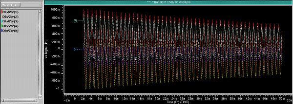
Example 1: NAND2 GATE

The HSpice simulation file is given by nand2.sp.
model : transistor model file (given in HSPICE tutorial)
netlist : circuit connection file (generated by layout parasitic extractor, e.g., PEX)
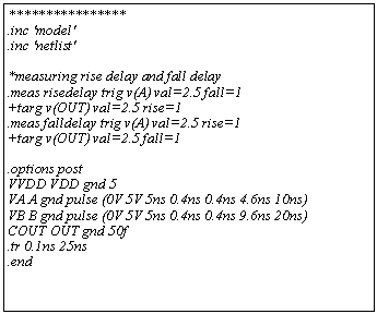
The simulation results are shown below.

From the simulation results, we have the correct functionality of the NAND2 gate. Now, you should be able to do your transient analysis. You might note that there are two .meas statements in the HSpice file, these two are for measuring the 50%-50% rise delay and fall delay. After running the simulation, you can look for these measurements in the *.mt0 file. If you want to have a symmetrical NAND2 gate or optimize the performance, you can use the sweep function provided by HSpice. Since parameters are specified in the netlist file, you can just add the following statements in your simulation code.
.tr 0.1ns 25ns sweep wn start_value stop_value increment
or
.tr 0.1ns 25ns sweep beta start_value stop_value increment
The first statement is for optimizing gate delays and the second one will help you to build a symmetric gate. The simulation results can be found in the *.mt0 file, you can choose the right parameter values base on the measured rise delays and fall delays. The optimizations are left to you as exercise.
Note: In some cases, you might want to specify some of the nodes in your circuits to some predefined values, in this case you can use the .IC command to do so. The general form for this command is given by:
.IC V(node1) val1 V(node2) val2 ...
Example 2: RC ladder
*transient analysis example
.options post
Vin 1 0 exp(0V 0.2V 2ms 20ms 40ms 20ms)
R1 1 2 3
R2 2 3 5
C1 2 4 7m
R3 4 0 8
C2 3 5 6m
R4 5 0 4
.tr 0.1ms 50ms
.alter Vin 1 0 pulse(0V 5V 5ms 0.5ms 0.5ms 4.5ms 10ms)
.alter Vin 1 0 sin(0 1V 1kHz 2ms 10 45)
.END
By exciting the source with different input waveforms, we have the following results.
exponential input

pulse input

sinusoidal input

5. DC Simulation
Syntax
The format for the .DC statement depends on the application in which it is used.
General forms
.DC var1 START=start1 STOP=stop1 STEP=incr1
.DC var1 START=[param_expr1] STOP=[param_expr2] STEP=[param_expr3]
.DC var1 start1 stop1 incr1 [SWEEP var2 type np start2 stop2]
.DC var1 start1 stop1 incr1 [var2 start2 stop2 incr2]
Examples
The following example causes the value of the voltage sources VIN to be swept from 0.25 volts to 5.0 volts in increment of 0.25 volts.
.DC VIN 0.25 5.0 0.25
The following example invokes a sweep of the drain to source voltage from 0 to 0V in 0.5V increments at VGS values of 0, 1, 2, 3, 4, and 5V.
.DC VDS 0 10 0.5 VGS 0 5 1
The following example asks for a DC analysis of the circuit from -55 to 125 degrees Celsius in 10 degrees Celsius increment.
.DC TEMP -55 125 10
As a result of the following script, a DC analysis is conducted at five temperatures: 0, 30, 50, 100, and 125 degrees Celsius.
.DC TEMP POI 5 0 30 50 100 125
In the following, a DC analysis is performed on the circuit at each temperature value, which results a linear temperature sweep from 25 to 125 degrees Celsius (five points), sweeping a resistor value called xval from 1k to 10k in 0.5k increments.
.DC xval 1k 10k .5k SWEEP TEMP LIN 5 25 125
Specification of the parameters:
incr1- voltage, current, element, model parameters, or temperature increment valuesnp- number of points per decade or per octave o just number of points depending on the preceding keyword.start1- starting voltage, current, element, model parameters, or temperature valuesstop1- final voltage, current, any element, model parameter, or temperature valuesSWEEP- keyword to indicate a second sweep has different type of variation (DEC, OCT, LIN, POI, ... )type- can be any one of the these: DEC, OCT, LIN, POIvar1- name of an independent voltage or current source, any element or model parameter, or the keyword TEMP (indicating a temperature sweep). Hspice supports source value sweep, referring to the source name.
Example
Let's say we want to explore the voltage transfer characteristic curve of the inverter shown below,

The transient analysis gives the following functionality curve.
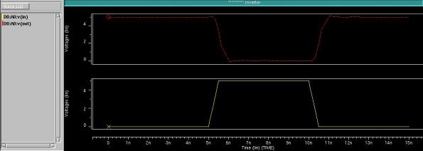
The VTC graph can be obtained by adding a DC analysis statement in the Hspice simulation file.
model : transistor model file (given in HSPICE tutorial)
netlist : circuit connection file (generated by layout parasitic extractor, e.g., PEX)
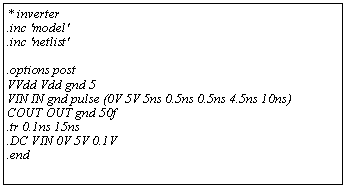
The curve is shown below:
