Young Research Group


Main menu:
The Young Research Group
The Young Research Group is engaged in investigating various inorganic, non-silicon-based semiconductors with high-k dielectrics for use in future nanodevice applications [e.g., transition metal dichalcogenides (TMDs), oxide-based and Group II-VI semiconductors, wide bandgap semiconductors, hafnium-based dielectrics, etc.]. We have collaborations within the MSE Department and externally as well.
Current Research
Large-Area/Flexible Electronics
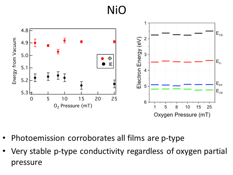
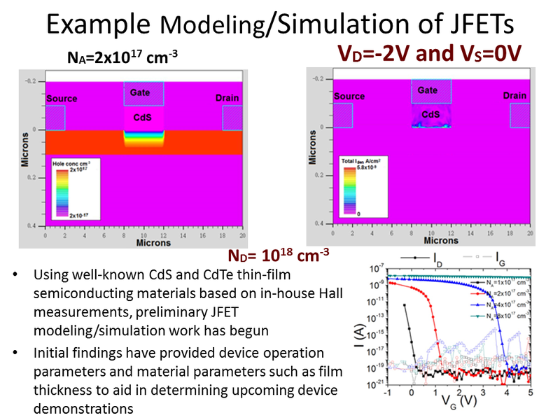
Large-area and/or flexible electronics are critical for the viability of some major aspects of the Internet of Things (IoT), medical, defense, and sensors applications. To accomplish this, new materials and devices, in particular, reliable thin-film transistor (TFT) technology are required to create circuitry. In this regard, a major technology challenge exists: suitable, low cost nanomanufacturing of inorganic, thin-film devices and circuits with integrated functionality. Therefore, we are investigating oxide- and chalcogenide-based inorganic semiconductors for use in conventional thin-film transistors and junction-based devices [e.g., metal/semiconductor and p/n junctions, junction field-effect transistors (JFETs)]. Currently, we are investigating n- and p-type materials that will evolve into viable device structures for performance and reliability evaluation.
Large-Area/Flexible Electronics Research


Click a thumbnail to enlarge
ß-Ga2O3
ß-Ga2O3 has emerged as a wide bandgap semiconductor with significant promise for power transistor applications due to the ability to operate at high frequencies and high voltage. This is due to its relatively wide bandgap (4.8 eV), and the larger Baliga's figure of merit relative to GaN and SiC. Moreover, ß-Ga2O3 can be grown as a single crystal material using a more cost-effective approach than SiC and GaN. Therefore, a systematic study of promising ß-Ga2O3 is needed to elucidate the fundamental response of the material in a metal-oxide-semiconductor (MOS) configuration for its potential future use in MOS high electron mobility transistors (MOS-HEMTs), which have attributes over conventional metal-semiconductor HEMT structures.
ß-Ga2O3 Research


Click a thumbnail to enlarge
Transition Metal Dichalcogenides
Transition metal dichalcogenides (TMDs) are under intense investigation due to their potential uses. We are investigating their use in future transistors as alternative channel materials because of their potential high mobility values while also providing robust on/off ratios. A majority of researchers are investigating relevant TMDs using bottom gate devices for the ease of integration. However, there have been very few studies to investigate the performance and reliability of top-gated FETs with high-k dielectrics on these TMD materials. Furthermore, the research on metal/TMD contacts is also important to improve the transistor performance. Therefore, we are engaging in the fundamental understanding of materials interactions at interfaces and this impact on performance and reliability for a device architecture that is commensurate with current CMOS fabrication approaches (i.e., top-gate FETs).
Transition Metal Dichalcogenides Research


Click a thumbnail to enlarge