To understand how any heterostructure device operates, one must be able to
visualize the energy-band profile of the device, which is simply a plot of
the band-edge energies  and
and  as functions of the position x.
These energies include the effects of the heterostructure energies
as functions of the position x.
These energies include the effects of the heterostructure energies  and the electrostatic potential
  . The electrostatic potential of course
depends upon the distribution of charge within the device
. The electrostatic potential of course
depends upon the distribution of charge within the device  .
In general,
.
In general,  depends upon the current flow within the device, and
the evaluation of a self-consistent solution for the potential, carrier densities
and current densities is the fundamental problem of device theory. However,
in many cases, one may obtain an adequate estimate of the band profile by
neglecting the current, and assuming that the device can be divided into
different regions, each of which is locally in thermal equilibrium with
a Fermi level set by the voltage of the electrode to which that region is
connected. We will refer to this as a quasi-equilibrium approximation.
Such calculations are readily performed on computers of very
modest capability. The formulation of the quasi-equilibrium problem of
course holds exactly in the case of thermal equilibrium (no bias voltages
applied to the device), and the equilibrium band profile of a heterojunction
has been studied by Chatterjee and Marshak [41]
and by Lundstrom and Schuelke [42].
depends upon the current flow within the device, and
the evaluation of a self-consistent solution for the potential, carrier densities
and current densities is the fundamental problem of device theory. However,
in many cases, one may obtain an adequate estimate of the band profile by
neglecting the current, and assuming that the device can be divided into
different regions, each of which is locally in thermal equilibrium with
a Fermi level set by the voltage of the electrode to which that region is
connected. We will refer to this as a quasi-equilibrium approximation.
Such calculations are readily performed on computers of very
modest capability. The formulation of the quasi-equilibrium problem of
course holds exactly in the case of thermal equilibrium (no bias voltages
applied to the device), and the equilibrium band profile of a heterojunction
has been studied by Chatterjee and Marshak [41]
and by Lundstrom and Schuelke [42].
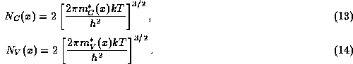
It is fairly common for heterostructures to create regions in which the carrier densities become quantum-mechanically degenerate. One therefore needs to take degeneracy into account in evaluating the carrier densities. We will assume that the energy bands are parabolic, so that the quasi-equilibrium carrier densities are

where  is the Fermi-Dirac integral of order
  ,
,

and the effective densities of states are
It is not particularly useful to express p and n in terms of the intrinsic density
 and the intrinsic Fermi level
  , because these quantities are not
constant throughout a heterostructure. (Formulations which emphasize these quantities
require the definition of an excessive number of auxiliary quantities to express the
content of the heterostructure equations [42,43].)
Also, the usefulness of
, because these quantities are not
constant throughout a heterostructure. (Formulations which emphasize these quantities
require the definition of an excessive number of auxiliary quantities to express the
content of the heterostructure equations [42,43].)
Also, the usefulness of  in the
elementary pn junction theory follows primarily from the mass-action law,
in the
elementary pn junction theory follows primarily from the mass-action law,
 , which is not valid in a degenerate semiconductor.
The net charge density includes contributions from the mobile carrier
densities  and
and  , and from the ionized impurity densities
 and
and  . If one takes into account the impurity statistics,
the ionized impurity densities will depend upon the potential:
. If one takes into account the impurity statistics,
the ionized impurity densities will depend upon the potential:

Here  and
and  are the degeneracy factors of the donors and acceptors,
respectively, and the impurity state energies
are the degeneracy factors of the donors and acceptors,
respectively, and the impurity state energies  and
and  are defined
with respect to the same energy scale as
are defined
with respect to the same energy scale as  .
The total charge density is then
.
The total charge density is then
Note that  depends upon
  ,
,  , and the band parameters
  and
and  through equations (1) and (1).
With the above expressions for the charge density, the electrostatic potential is described by Poisson's equation, plus the appropriate boundary conditions. In a heterostructure, the dielectric constant will typically vary with semiconductor composition, so Poisson's equation must be written as
This form guarantees the continuity of the displacement. The screening equation for
a heterostructure is obtained by combining all of the equations in this
section into (18). It is a nonlinear differential equation
for  , as the materials parameters are fixed by the design of the
heterostructure, and the Fermi levels are fixed by the external circuit.
The solutions to this nonlinear equation are well behaved and stable, however,
because the charge density varies monotonically with
, as the materials parameters are fixed by the design of the
heterostructure, and the Fermi levels are fixed by the external circuit.
The solutions to this nonlinear equation are well behaved and stable, however,
because the charge density varies monotonically with  and has the
screening property: making the potential more positive makes the charge
density more negative and vice versa.
and has the
screening property: making the potential more positive makes the charge
density more negative and vice versa.
The boundary conditions to be applied to this screening equation follow
from the condition that each semiconductor material must be charge-neutral
far from the heterojunction. Let the boundary points be  and
and  .
These can be taken to be
.
These can be taken to be  if one is solving for the potential
analytically, but if numerical techniques are used
if one is solving for the potential
analytically, but if numerical techniques are used  and
and  should be
finite but deep enough into the bulk semiconductor that charge neutrality
may be assumed. One then determines
should be
finite but deep enough into the bulk semiconductor that charge neutrality
may be assumed. One then determines  and
and  simply by
solving
simply by
solving

The physical picture that is assumed in this formulation is that the
Fermi energy (possibly different in different regions of the device) is
set by the voltages on the terminals of the device. The terminals, together
with the circuit node to which they are connected, are charge reservoirs
whose chemical potential is just the Fermi level. The device and the
circuit exchange charge, and the entire energy band structure, floats
up or down until charge neutrality in the bulk is achieved. Thus the
origin of the scale of  is set by the combined choice of the energy
scale for the band-structure energies
is set by the combined choice of the energy
scale for the band-structure energies  and
and  , and the choice of
ground potential for the circuit voltages (and thus the Fermi levels).
The Fermi energies on each side of the junction
, and the choice of
ground potential for the circuit voltages (and thus the Fermi levels).
The Fermi energies on each side of the junction
 are determined by the externally applied voltages at the respective contacts.
In fact, it is most convenient to define the Fermi energy with respect to
the circuit ground potential so that
are determined by the externally applied voltages at the respective contacts.
In fact, it is most convenient to define the Fermi energy with respect to
the circuit ground potential so that

where  is the voltage of the circuit node connected to the i'th
device terminal.
is the voltage of the circuit node connected to the i'th
device terminal.
If the carrier densities are
neither degenerate nor closely compensated, the Fermi functions in
(1) may be approximated by exponentials and one may
directly solve for  to obtain the more familiar expressions:

The diffusion voltage, which appears in the standard pn junction analysis, is just
the magnitude of the potential difference across the heterojunction
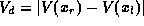 .
.
The screening equation consisting of Poisson's equation (18)
combined with the charge density expression (17) and subject
to the boundary values obtained by solving (1) is a
nonlinear differential equation for the electrostatic potential  .
It is best solved numerically for each specific case, due to the large number
of band alignment topologies. An effective approach is to make a
finite-difference approximation to the equation, reducing it to a set of
simultaneous nonlinear algebraic equations, and solve these using
Newton's method (see Selberherr [44]). The examples presented below were calculated using this approach.
.
It is best solved numerically for each specific case, due to the large number
of band alignment topologies. An effective approach is to make a
finite-difference approximation to the equation, reducing it to a set of
simultaneous nonlinear algebraic equations, and solve these using
Newton's method (see Selberherr [44]). The examples presented below were calculated using this approach.
If a given heterojunction is doped so as to achieve the same conductivity type on both sides of the junction (n-n or p-p), the junction is said to be isotype. If opposite conductivity types are achieved (p-n or n-p), it is an anisotype junction. Figures 13--15 illustrate a few of the many possible band profiles that can be obtained with heterojunctions.

Figure 13: Self-consistent band profile of an anisotype straddling heterojunction
in equilibrium. The In Ga
Ga As-InP
heterojunction was chosen to emphasize the band discontinuities.
As-InP
heterojunction was chosen to emphasize the band discontinuities.
Figure 13 shows the band profile of an anisotype straddling junction in equilibrium. Apart from the band-edge discontinuities the profile resembles that of a pn homojunction.

Figure 14: Self-consistent band profile of an isotype heterojunction under a
small reverse bias. Again the In Ga
Ga As-InP is shown.
An isotype junction is shown in Fig. 14. Its band profile resembles that of a Schottky barrier. Figure 15 shows the profile of a broken-gap system. The bands are fairly flat, despite the fact that this is an anisotype junction.
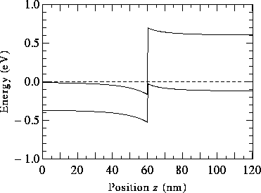
Figure 15: Self-consistent band profile of a broken-gap
(N)InAs-(P)GaSb heterojunction in equilibrium.
This doping configuration is the most easily fabricated.